The advancement of semiconductor manufacturing techniques, moving to ever smaller process nodes, do not only benefit flashy CPUs, GPUs and SoCs. These gains also reach the embedded world, where MCUs dominate. Although usually several generations behind, microcontrollers eventually adopt “new” processes, bringing big advantages: more powerful cores, more advanced peripherals, and still in tiny, low-power packages.
Today’s most advanced MCUs are build on nodes from a few years ago, e.g. STMicroelectronics uses 16 nm FinFET, Renesas an optimized 22 nm, and NXP a 28 nm FD-SOI. These nodes not only allow larger and faster clocking processing cores but also faster and more advanced peripherals. However, they also come with a trade-off: incompatible with embedded Flash. As a result, these MCUs now require external Flash memory.
Some of the new features these MCUs gained over the years, once exclusive to their bigger cousins the microprocessors (SoC), include 2D/2.5D graphics accelerators and LCD controllers. Now they arrived at the next step, slowly integrating advanced camera interfaces and image/video accelerators. While parallel camera interfaces have existed for years, a few MCUs now include a full MIPI CSI-2 interface, the same standard found in microprocessors powering SBCs like the Raspberry Pi, or in smartphones. This opens up the enormous ecosystem of modern image sensors to the MCU world.
To handle the high throughput of MIPI CSI-2, some of these MCUs also integrate hardware image and video encoders:
- JPEG encoders for still images.
- H.264 (MPEG-4/AVC) video encoders for HD streaming.
Currently, these encoders typically support Full HD (1080p) at “cinema-grade” frame rates of up to 30 fps. Below is a list of currently (as of September 2025) available MCUs with MIPI CSI-2 camera interfaces from all major manufacturers:
| Parameters | STM32N6 | ESP32-P4 | i.MX RT1170 | RA8P1 | Units |
|---|---|---|---|---|---|
| Core | Cortex-M55 | Dual RISC-V | Cortex-M7 + M4 | Cortex-M85 + M33 | |
| Clock | 800 | 360 | 1000 + 400 | 1000 + 250 | MHz |
| Performance | 3360 | 2489 | 6468 | 7300 | CoreMark |
| SRAM | 4200 | 768 | 2000 | 2000 | kByte |
| Flash | External | External | External | External | kByte |
| MIPI CSI-2 | 2-Lane 2.5G | 2-Lane 1.5G | 2-Lane 1.5G | 2-Lane 720M | |
| ISP | 5MP 30fps | 2.1MP 30fps | NA | 8MP | |
| VENC (H.264) | 1080p30 | 1080p30 | NA | NA | |
| JPEG | 300 MP/s | 1080p40 | NA | NA | |
| NPU | 600 | NA | NA | 256 | GOPS |
| SDMMC | 104 | 25 | 104 | 25 | MByte/s |
| Int. USB | 480 (HS) | 480 (HS) | 480 (HS) | 480 (HS) | MBit/s |
| Ethernet | 10/100/1000 | 10/100 | 10/100/1000 | 10/100/1000/2500 | MBit/s |
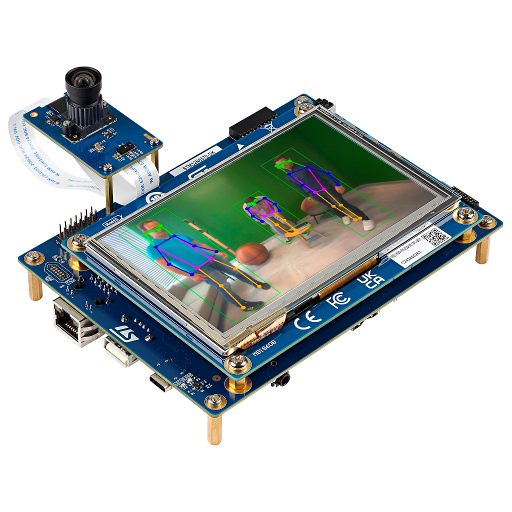
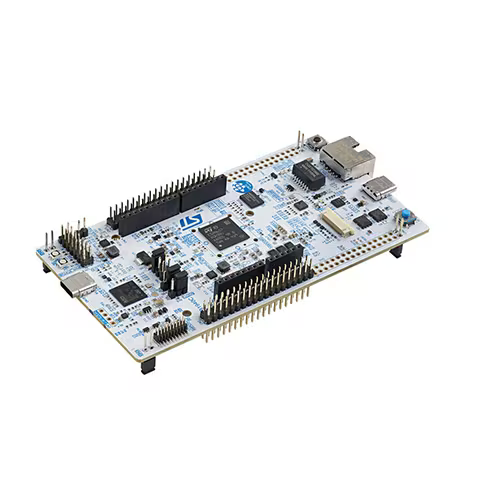
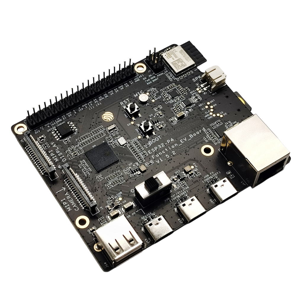
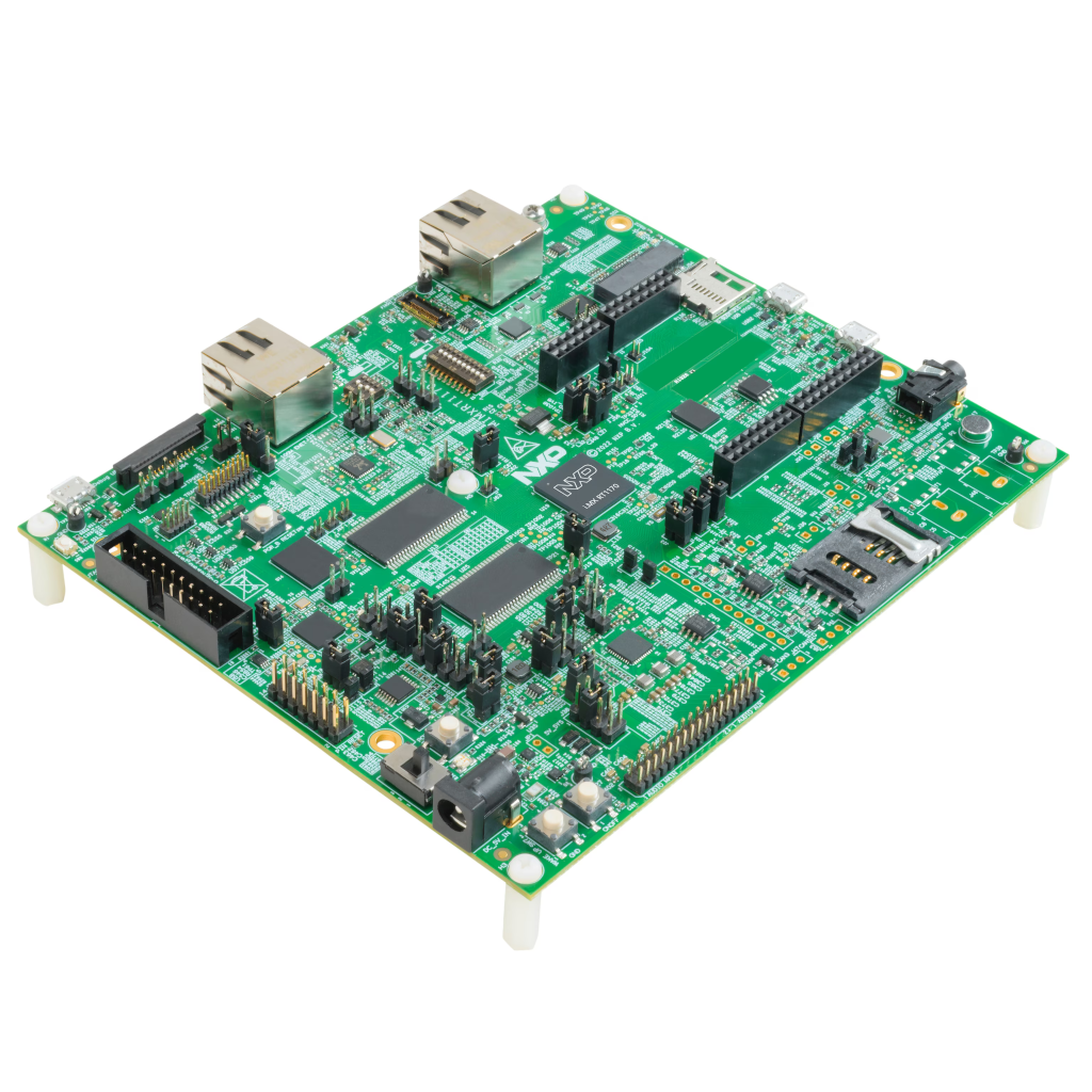
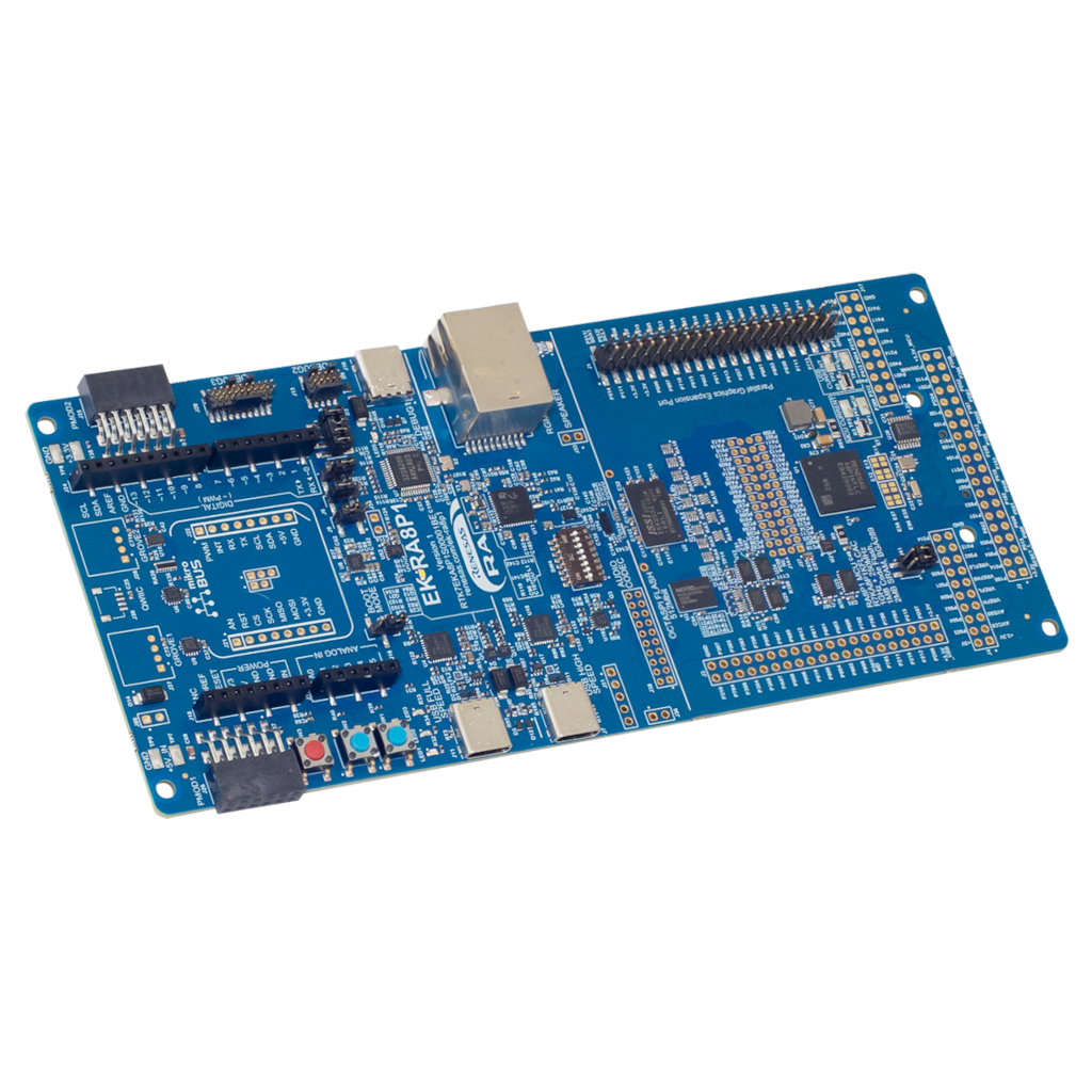
First we have the newest MCU family from STMicroelectronics, the STM32N657X0 launched in early 2025 with its accompanying development board (not the more complex evaluation board), the NUCLEO-N657X0-Q. Next we have the first MCU only, with no WiFI/BLE, chip from Espressif, the ESP32-P4 which launched also in early 2025 and also has a simple development board, the ESP32-P4-Function-EV-Board. Next is the oldest of them, the i.MX RT1170 from NXP launched back in 2020 with a larger and more complex development board, the i.MX RT1170 EVKB. Finally, we have the newest MCU family from Renesas, the RA8P1 launched closer to mid 2025 with a simple development board, the EK-RA8P1.
Video/Image Encoder
Of the listed MCUs, only two currently include dedicated video/image encoders: the STM32N657X0 and the ESP32-P4. Both support JPEG encoding/decoding for sill and dynamic images, as well as a hardware video encoder (VENC) supporting the H.264 format.
For JPEG, the STM32N6 has higher theoretical raw throughput with up to 300 MPixel/s, compared to the ESP32-P4’s ~83 MPixel/s (listed in the datasheet as 1080p @ 40 fps). For H.264 (MPEG-4 Part 10/AVC), both MCUs officially support 1080p30, though actual performance may vary with compression profiles (Baseline/Main/High). This remains to be seen and tested when I get them in my hands and have time for it.
ST provides more documentation of their H.264 encoder, the STM32N6 Reference Manual details the encoder’s bitrate range (10 Kbit/s to 40 Mbit/s) and supported image sizes (96×96 up to 4080×4080). Interestingly, in JPEG mode it supports images as large as 8176×8176 when sourced from RAM, though the integrated ISP is limited to 2688x1944 (5 MP). Espressif’s ESP32-P4 documentation is not yet providing full details, with almost no information on the H.264 encoder in there reference manual or datasheet.
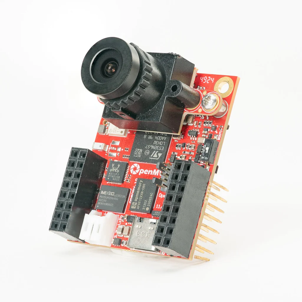
Besides the MIPI CSI-2 interface, the ISP, and the hardware encoders, the STM32N6 also integrates a proprietary in-house-developed NPU (Neural Processing Unit) with up to 600 GOPS. A perfect companion for lightweight image recognition and computer vision tasks on the edge. Thanks to this rich feature set, the STM32N6 is already starting to appear beyond ST’s own ecosystem. For me most interestingly by OpenMV, launching the new OpenMV N6. This new board lunched with a successful Kickstarter campaign and is expected to start shipping to backers in December 2025.