
The PlumaN6 HD is a custom embedded controller designed for drone and robot control. Its primary target is the custom Lince N6 wheeled robot.
The controller follows a “bare-metal” design philosophy, extracting maximum performance and features from an MCU platform without relying on a Linux SBC. At its core is the STM32N6, enabling a single-chip solution for both the motion control and vision stacks. The project focuses on taking this new architecture to its limits, experimenting with applications where this no-SBC architecture can replace the traditional “Raspberry Pi (SBC) + MCU” architecture.
The key specifications for the PlumaN6 HD are:
- MCU: STM32N6 (Cortex-M55 @ 800 MHz + Neural Art NPU @ 1 GHz / 600 GOPS)
- Memory: 4.2 MB internal SRAM, Octa-SPI Flash (up to 400 MB/s), Hexa-SPI PSRAM (up to 800 MB/s), Micro-SD UHS-I.
- Vision Pipeline: 2-Lane MIPI-CSI (2.5 Gbps/lane), DCMI (8-bit parallel), Hardware ISP (5 MP), H.264 Hard Encoder (1080p), JPEG Codec.
- High Speed Comms: 1000Base-T1 Automotive Ethernet (1 Gbps), USB 2.0 HS (480 Mbps).
- Real-Time I/O: 3x CAN-FD, 4x I2C FM+, 2x I3C (12.5 MHz), 4x SPI, 5x UART.
- Sensors (6-DoF): On-board IMU (Accel/Gyro/Mag/Baro). Dedicated port for External Redundant IMU (Heated, Vibration Isolated).
- Wireless: On-board ESP32-C5 (Dual-Band WiFi 6 + Bluetooth LE). Expansion headers for RC/Telemetry (e.g. ELRS).
- Power Input: 6V–30V Wide Input (for 2S to 7S LiPo). Integrated Current/Voltage monitoring on the 5V rail for system telemetry.
⚠️ Note: This project is in active development. Specs and features are subject to change as I validate the design.
Project Status: 🚧 In Fabrication (Rev A). Follow for project updates on Twitter/X or Bluesky.
Version History
Revision 1 (Rev. A)
Schematic: PlumaN6_Schematic_RevA.pdf
Gerber: PlumaN6_Gerber_RevA.zip
The PlumaN6 HD board is in the first version (Rev. A). This version has a few hardware mistakes, listed below for reference:
- SDMMC VDDIO: SDMMC1 and SDMMC2 have there IO voltage connections switched i.e. the supply for SDMMC1 is connected to VDDIO5 (wrong) instead of VDDIO4 (correct).
- uSD Card Interface: The IOs used for the SDMMC1 interface, to the uSD card, are not all on the primary GPIOs i.e. D0 is connected to the alternative GPIO PD11 which is not in the VDDIO4 domain.
- PA8 should be kept as reserved as it is the default BOOT1 pin (used for debug mode). This can be OTP changed to any GPIO though.
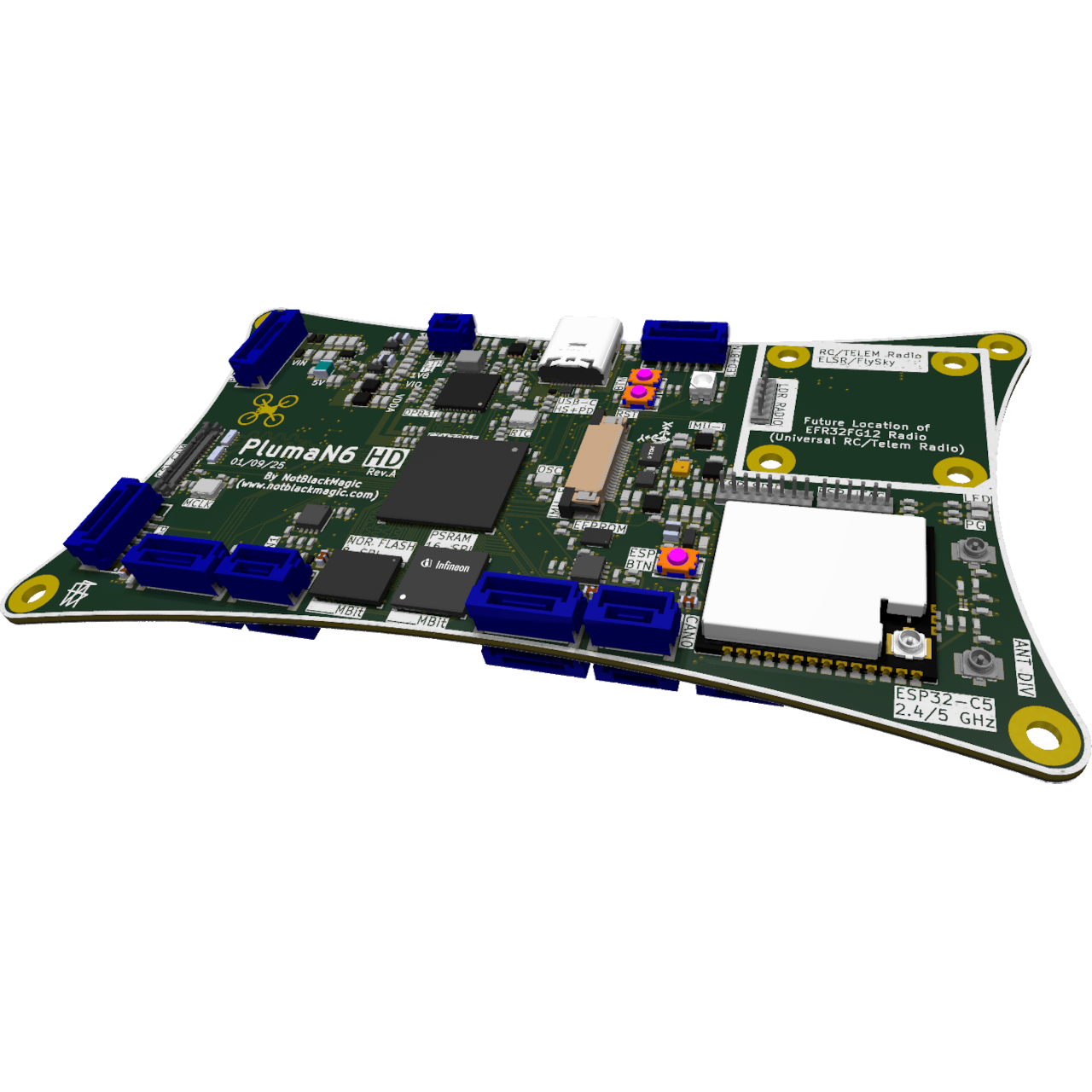
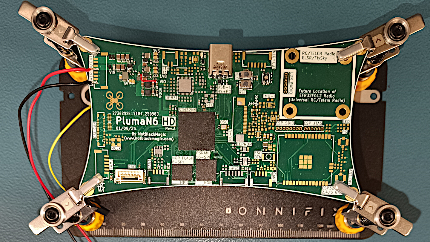
Overview
Below is a view of the PlumaN6 HD board with the location of the different functional modules:
Power Supply
The PlumaN6 features a relatively complex power architecture. The STM32N6 requires multiple independent supplies and some power up sequencing. Additionally key peripherals and sensors have their own supply rail (e.g. the IMUs, Radio, Micro SD card, etc…). Below is a block diagram overview of the complete power supply scheme:
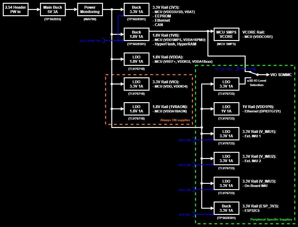
The main power input is through a JST-GH connector, accepting a wide 6 V to 30 V range (2S to 7S LiPo). This input feeds a high-efficiency TPS62933 3 A buck converter, generating the primary 5 V backbone for the whole board. This is followed by an INA700 power monitor, providing real-time voltage and current readings of the main rail.
The STM32N6 is powered by five distinct rails plus its integrated SMPS for the core voltage. There are two high-power rails: a 3.3 V rail (shared with Ethernet/CAN) and a 1.8 V rail (for the core SMPS, HyperFlash, and HyperRAM). Crucially, both these high power rails are gated by the MCU, and not powering up automatically. Alongside the high-power rails, there are three low power LDO rails: a 1.8 V rails for the analog domain and some IOs, and both a 3.3 V and 1.8 V rails for some IOs as well as the always ON required supplies.
Besides the MCU domain, there are dedicated 3.3 V rails for the three IMU channels, one for the on board and two to the offboard sensors. The high speed radio, ESP32-C5 module, has its own high-power 3.3 V rail. Finally there is a 1 V rail for the Automotive Ethernet IC and a 3.3 V rail dedicated to the Micro-SD card supply.
Microcontroller and Memories
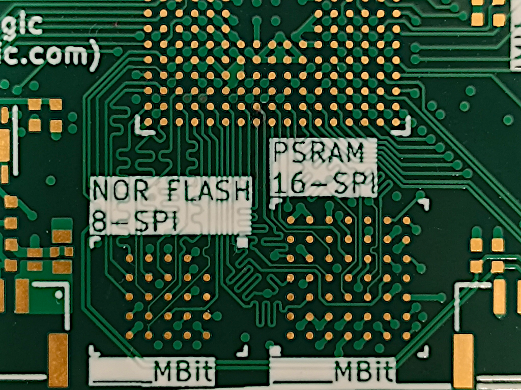
Because the STM32N6 is flashless, an external non-volatile memory is strictly required for firmware storage and execution. Additionally, for high resolution vision tasks and NPU workloads, the large internal SRAM is not sufficient and has to be extended. Due to this, the PlumaN6 relies on two high-performance external memory devices:
- Flash: 64 Mbyte Infineon HyperFlash
- RAM (PSRAM): 32 MByte Infineon HyperRAM (space for up to 7 raw 1080p frames)
Both of these external memories connect to the MCU via HyperBus, the highest-performance memory interface available on the STM32N6, and can operate in memory-mapped mode. The Flash utilizes an 8-bit wide bus, while the PSRAM operates over a 16-bit wide bus. When running at the maximum clock speed of 200 MHz in dual-rate mode, this architecture can reach a theoretical throughput of up to 400 MB/s for the Flash and up to 800 MB/s for the PSRAM. To support the maximum 200 MHz clock, the HyperBus peripheral is driven at 1.8 V via the STM32N6’s independent IO domains (VDDIO2 and VDDIO3).
The MicroSD card connects over a 4-bit wide SDMMC interface. To support UHS-I speeds with clocks exceeding 50 MHz, the IO voltage must be switched to 1.8 V. This can be achieved with an external level translator or by exploiting the dedicated IO supply for the SDMMC interfaces (VDDIO4 for SDMMC1 and VDDIO5 for SDMMC2). Using the dedicated supply requires that all I/O pins for the interface connect to primary, non-alternate pins controlled by that specific domain. This routing constraint was overlooked in Rev. A of the board, where the SDMMC1 D0 pin was connected to an alternate GPIO (PD11) instead of the primary pin (PC8), placing it outside the VDDIO4 supply domain. Due to this, the MicroSD interface on the Rev. A prototype is limited to 3.3 V speeds (up to 50 MHz clock), with full UHS-I capabilities planned for the next board revision.
Routing for both the SDMMC and HyperBus interfaces follow the guidelines provided by STM (AN5967). The main constraints to look out for are:
- Trace lengths as short as possible (recommended to be below 120mm)
- Clock to data lane length skew below 10 mm (trace length matched as best as possible)
- Only routed on Top or Bottom layer with GND reference layer beneath
- Impedance matched traces to 50 Ohm
This optimized HyperBus layout is shown in the figure below:
Vision System
One of the standout feature of the STM32N6 is its advanced vision architecture, featuring a hardware ISP, MIPI-CSI interface, and H.264 video encoder (VENC), where the motivation behind developing the PlumaN6. To fully leverage these capabilities, the PlumaN6 features two distinct camera interfaces:
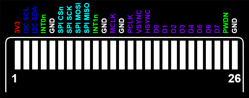
- SD Camera (Optical Flow): A parallel DCMI interface on a 26-pin FFC/FPC connector, intended for lower-resolution sensors used in optical flow and navigation.
- HD Camera (Imaging/AI): A high-speed MIPI-CSI interface on a 26-pin DF56C connector, intended for high-resolution imaging, object detection, and video capture.
The SD camera interface uses the legacy parallel DCMI interface, compatible with widely available older sensors like the OV7670, OV2640 or OV5640. On the PlumaN6 it supports a 8-bit bus width at speeds up to 80 MHz. Besides the DCMI, the connector includes I3C and SPI buses, intended for future high-bandwidth auxiliary sensors (e.g., LiDAR). The pinout is shown below:
The HD camera interface uses the high bandwidth serial MIPI-CSI peripheral, supporting 2 lanes at up to 2.5 Gbps per lane. This interface is compatible with most modern sensors limited primarily by the MCU’s internal processing throughput.
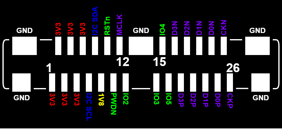
The interface uses a 26-pin DF56C connector, allowing for flexible, robust cabling ideal for gimbal-mounted sensors. The pinout was designed with the intention of being compatible with some existing FPV camera systems (specifically the DJI O3/Air Unit cameras), though this is completely untested and based only on this. In addition to the MIPI-CSI interface, the connector also carries a I3C and four GPIOs, enabling direct control of gimbals and high-bandwidth auxiliary sensors. The pinout is shown below:
Sensors
The PlumaN6 is designed as a high-performance robotics and drone controller board. For this, it features a complete on-board 10-DOF sensor set alongside a specialized interface for an external, redundant sensor module. The on-board sensor set is composed of:
- 6-Axis IMU: LSM6DSO (3-Axis Accelerometer + 3-Axis Gyroscope)
- 3-Axis Magnetometer: LIS2MDL
- Barometer: ICP-20100
To ensure the lowest latency and achieve the highest sample rates for fast real-time control loops, the high-rate 6-Axis IMU is connected via a dedicated SPI bus. The lower-rate magnetometer and barometer are routed over a shared I2C bus. Finally, the on-board sensor block includes a 1 Kbit I2C EEPROM (24FC01) for non-volatile storage of sensor calibrations, offsets and other relevant information.
In addition to these on-board sensors, the PlumaN6 exposes a 20-pin FFC/FPC connector designed to connect with a custom external sensor board. The pinout is shown below:
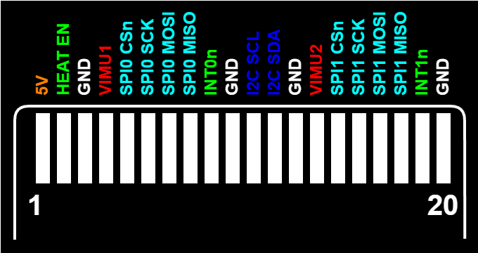
The connector provides two independent power supplies, two dedicated SPI buses, and a single I2C bus. It also features a dedicated hardware control line intended to drive a heater transistor on the external board. This allows the external IMU array to be maintained at a constant temperature, guaranteeing thermal calibration stability across different ambient conditions.
Wired Connectivity
The PlumaN6 features an extensive set of wired connectivity options, which can be divided into standard control interfaces and a high-bandwidth interfaces. The standard control interfaces are mapped to JST-GH connectors around the edge of the board, following the Pixhawk standard pinouts. This ensures compatibility with the existing drone hardware ecosystem. These interfaces include:
- 3x CAN-FD: Utilizing TJA1462 SIC transceivers.
- 2x GPS Ports: Carrying both UART and I2C signals.
- 2x Telemetry Ports: Carrying UART with hardware flow control.
- 1x I2C & 1x I3C: For external peripheral expansion.
- 8x PWM Outputs: On two independent 4-channel headers for servos, ESCs, and actuators.
These standard connections provide comprehensive support for external hardware, from GPS and speed sensors to motor controllers.
On the high-bandwidth side, the PlumaN6 stands out among other MCU-based controller boards. It provides a full High-Speed USB 2.0 (480 Mbps) interface via a USB-C connector. Furthermore, the board features a Gigabit Automotive Ethernet interface (1000BASE-T1) powered by the DP83TG721 transceiver and operating over a single twisted pair on a JST-GH connector. These two itnerfaces allow the PlumaN6 to interface with a companion Single Board Computer (SBC), or another PlumaN6 board, with sufficient throughput to simultaneously stream real-time telemetry, raw camera frame data, and other high-bandwidth sensor signals.
To fully exploit the performance limits of the STM32N6, the PlumaN6 HD is powered by Instinct, a custom-developed C++ firmware stack. In an effort to increase performance, and improve my knowledge of the hardware and MCU architecture, Instinct does not use standard abstraction layers (like the ST HAL). Instead, it relies on fully custom bare-metal peripheral drivers utilizing direct register access and Low-Layer (LL) APIs.
Stack
Instinct is built around a highly modular design using Eclipse ThreadX as the RTOS, alongside companion modules like FileX for high-speed storage management. At the core of this modularity is a custom Publish-Subscribe (PubSub) messaging architecture (inspired by PX4 uORB, uROS and similar projects). This acts as the central messaging system of the firmware, passing data between decoupled sensor acquisition threads, state estimators, and control loops, with planned bridges to micro-ROS (uROS) and MAVLink.
Open Source Development
Although Instinct is purpose-built for the PlumaN6 HD, its decoupled driver structure allows core components to be easily ported to other custom STM32N6 hardware designs.
The firmware is completely open-source and licensed under the GNU GPL-3.0. As the PlumaN6 HD hardware validation continues, the codebase is under active, heavy development.
The full firmware is available on GitHub: Instinct
Current Phase: 🧩 Board Bring-up & Driver Development
Last Updated: March 11, 2026
The majority of the hardware manufacturing phase for Revision A is complete, and the board is currently on the bench for validation.
Initial bring-up has been successful: all power rails are stable, and the STM32N6 is correctly executing code (currently only in debug mode and running from SRAM). The focus is now on the Instinct firmware, specifically in writing the bare-metal drivers for external memory (HyperBus) and other peripherals, with no reliance on HAL when possible.
Timeline:
- Next: USB-HS driver and USB device classes, custom driver and maybe also USBX.
- 2026-03-11: Started driver development for USB-HS peripheral.
- 2026-03-08: Integrated FileX with SD card driver.
- 2026-03-05: SD card driver implemented and tested with C10 class card (5 MByte/s read and 18.7 MByte/s write).
- 2026-02-26: SDMMC driver tested and working up to 50 MHz (due to hardware error no 1.8 V level speeds).
- 2026-02-18: HyperBus tested and working up to 100 MHz.
- 2026-02-11: Started driver development for HyperBus devices: HyperRAM and HyperFlash.
- 2026-02-04: Basic UART driver, Logger and Console/Shell implemented.
- 2026-02-02: First “Hello World” program running on MCU.
- 2026-01-30: Milestone: Minimal assembly achieved, power rail validated and first MCU discovery.
- 2026-01-25: BGA soldering, MCU, Flash and PSRAM.
- 2026-01-23: PCBs and stencils arrived!
- 2026-01-12: Started on project documentation and landing page.
- 2026-01-04: PCBs ordered.
- 2025-11-08: Milestone: Layout frozen.
- 2025-09-01: Rev A Schematic defined.
- 2025-06 to 2025-08: Architecture defined (STM32N6, Memory, T1 Ethernet, Sensors, etc…).
Experimental Hardware This board is a “First Prototype” design. Features, pinouts and functionalities are subject to change as I validate the board design and develop the firmware.
I am planning on documenting the assembly and debugging process in “real-time”: