The STM32N6 represents a significant shift in STMicroelectronics’ MCU lineup. It is ST’s first implementation of the Arm Cortex-M55 core, but more significantly, it introduces a dedicated NPU, specifically STMs’ custom Neural-ART Accelerator, alongside MIPI-CSI, a 5 MP ISP, and a H.264 hardware encoder (VENC). At the time of release, this makes it one of only two MCUs with a native H.264 encoder. To top it of, it integrates a STM Neo-Chrome 2.5D GPU, a USB High-Speed (480 Mbps) controller and PHY, and a 1-Gbit Ethernet interface.
This huge variety of peripherals and hardware accelerators makes the STM32N6 one of the most versatile MCUs on the market right now. The core itself runs at up to 800 MHz, reaching 1280 DMIPS and a 3360 CoreMark score. while the NPU runs at up to 1 GHz to provide 600 GOPS at an efficiency of 3 TOPS/W. To feed both the NPU and VENC pipelines, a massive internal SRAM of 4.2 MByte is embedded, expandable externally through FMC or XSPI/HyperBus interfaces.
The downside of this complex MCU is that it is flashless, requiring an external flash for the firmware. Additionally, managing this volume of complex peripherals alongside the security extensions (TrustZone, secure IO, and isolated memory access) introduced by the Cortex-M55 makes bare-metal system initialization no easy feat.
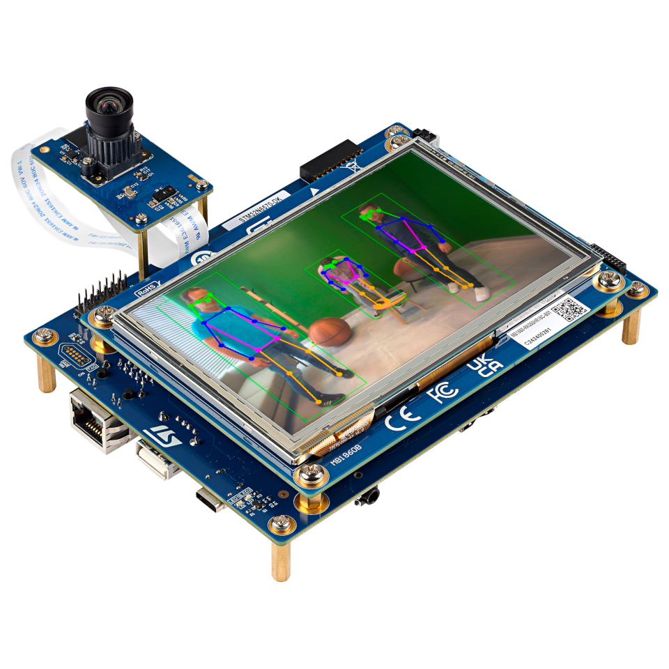
This page serves as a “Living Notebook” for implementation details, gotchas, and lessons learned while implementing bare-metal peripheral drivers for the STM32N6. These insights were/are gathered during the development of the Instinct firmware for the PlumaN6 HD robot controller. This is not a in-depth tutorial series, but rather a collection of architectural traps, implementation details and gotchas to take into account when developing for the STM32N6 and pushing it to its limits.
Power Domains
The increased complexity of the STM32N6 starts with the power supply scheme. The MCU requires multiple independent supplies and some strict power-up sequencing. At a minimum, three different rails are required:
- VDDA18AON (1.8 V): Supplies the core analog blocks, oscillators, and power management. This is an “Always-On” rail and must be provided first.
- VDD (3.3 V or 1.8 V): Supplies the standard I/Os.
- VDDCORE (typically 0.8 V): Powers the internal functional logic (e.g. the CPU core). This can be generated by the integrated SMPS or provided externally.
Furthermore, some peripherals (such as USB, CSI, ADC, and the PLLs) have dedicated supply pins that can be tied to one of these three main supplies.
To support high-speed interfaces without external level shifters, the STM32N6 features dedicated, independent supplies for specific I/O banks:
- XSPI/HyperBus: Powered by VDDIO2 (pins PO[5:0] and PP[15:0]) for XSPIM1, and VDDIO3 (pins PN[12:0]) for XSPIM2.
- SDMMC: Powered by VDDIO4 (pins PC[1], PC[12:6] and PH[9,2]) for SDMMC1, and VDDIO5 (pins PC[0], PC[5:2] and PE[4]) for SDMMC2.
It is important to note that to use these dedicated IO voltage supplies, the peripheral signals must be routed to their primary IO pins! If you route an SDMMC signal to an alternate pin (e.g., mapping D0 to a pin outside the VDDIO4/5 groups), that pin will be driven by the main VDD rail instead.
Below is a block diagram of the supply scheme used to power the STM32N6 MCU in the PlumaN6 HD board:
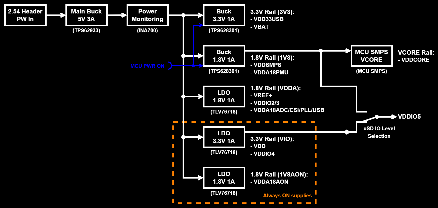
In this scheme, VDDCORE is generated by the integrated SMPS, which itself is powered by a 1.8 V rail. The VDD, VBAT, and VDD18AON rails are powered by always-on LDOs, while the remaining supplies are connected to supplies with their EN controlled by the MCUs Power-On signal. The non-dedicated IOs are powered by a 3.3 V rail. The dedicated IO supplies for the XSPI/HyperBus (VDDIO2 and VDDIO3) are powered by a 1.8 V rail, while the SDMMC interface to the uSD card uses a dynamic supply switch to toggle between 3.3 V (for initialization) and 1.8 V (for UHF-I speeds).
Clocks & PLLs
The clock tree of the STM32N6 is also significantly more complex and configurable than previous STM32 families. It keeps the multiple clock sources and oscillators (HSE, HSI, MSI, LSE, LSI) but expands the clock tree with 4 independent PLLs (PLL1 to PLL4) and 20 distinct clock dividers (IC1 to IC20). These ICx dividers take a PLL output and scale it down for specific domains:
- IC1: CPU core clock (SYSA)
- IC2: AXI, AHB, and APBx buses (SYSB)
- IC6: Neural-ART NPU clock (SYSC)
- IC11: Tightly coupled NPU SRAM (AXISRAM3/4/5/6 via SYSD)
The remaining dividers are used for peripheral groups (e.g., all I2Cs or all UARTs share a divider). There are although some nuances here, and which are “hidden” in the STM32CubeMX configuration. For instance, the CSI-PHY clock is IC18, which must be manually enabled and set to a maximum of 27 MHz.
An interesting challenge is running all high-speed cores at their respective maximum clocks. This is, the MCU core at 800 Mhz, the NPU core at 1000 MHz, and the NPU SRAM (AXISRAM3/4/5/6) at 900 MHz. Because there is no low enough common multiple between these frequencies, they cannot be derived from a single PLL. On the PlumaN6, this is solved by dedicating a PLL to each major domain:
- MCU Core: PLL1 (VCO at 3200 MHz, divided by 4 = 800 MHz)
- NPU Core: PLL2 (VCO at 3000 MHz, divided by 3 = 1000 MHz)
- NPU SRAM: PLL3 (VCO at 2700 MHz, divided by 3 = 900 MHz)
Although this might come with performance penalties for data crossing different clock domains/speeds, this has not been evaluated yet. The complete implementation for this clock configuration can be found in the Instinct firmware repository here.
Boot & Security
Section under development with content to come!
One of the most radical architectural changes in the new STM32N6 series is that it is entirely flashless, requiring external flash memory to store and execute firmware. To support this, the MCU features a highly versatile set of memory interfaces including a parallel FMC (Flexible Memory Controller), two high-performance XSPI (Extended Serial Peripheral Interface) ports compatible with up to 16-bit wide HyperBus protocols, and dual SDMMC interfaces.
These interfaces are also available in other STM32 MCU series but are crucial in the STM32N6, not just for the firmware, but for expanding the RAM buffers for the NPU and video pipeline. To get the maximum performance out of the Cortex-M55 core, NPU, and video stack, the highest bandwidth interface must be used. At first glance, one might assume that this is the parallel FMC, but this is not the case. The highest bandwidth interface available is the XSPI running in a 16-bit wide HyperBus configuration. It reaches a theoretical throughput of 800 MByte/s (200 MHz clock, 16-bit wide, double data rate) compared to the 664 MBytes/s of the parallel FMC (166 MHz clock, 32-bit wide, single data rate). The STM32N6 provides two HyperBus compatible ports: one 16-bit wide and one 8-bit wide. On the PlumaN6 HD board, the 16-bit port is dedicated to external high-speed PSRAM, while the 8-bit port handles external Flash.
This section focuses on the direct-register implementation details and hardware-level gotchas encountered while building the HyperBus and SDMMC drivers.
HyperBus
The XSPI peripheral operating in HyperBus protocol mode is relatively straightforward to initialize, even though it is one of the few peripherals that lacks an LL driver abstraction from ST. Because ST only provides a HAL implementation, you have to extract the raw register configurations manually. The essential register steps match previous STM32 families, but a few things require close attention:
- Symmetric Clocking: The clock prescaler register value should be an odd number to achieve an even division factor, ensuring a symmetric duty cycle clock signal.
- Minimum Access Granularity: Read and write transactions depend on bus width. On an 8-bit HyperBus, the minimum access is 16-bit; on a 16-bit bus, it is 32-bit. This is especially important when modifying internal registers of external devices.
- Byte vs Word Addressing: The STM32N6 XSPI peripheral handles addressing at the byte level. However, most external HyperBus devices expect word-aligned addressing. The driver must handle this conversion.
- Latency Restrictions: When operating in 16-bit HyperBus mode, the STM32N6 does not support variable latency configurations. Both the peripheral and the external device must be configured to fixed latency.
When using HyperBus memory areas via DMA rather than memory-mapped mode, standard cache coherency rules apply: invalidate the D-Cache before a read and clean (flush) the D-Cache after a write. Finally, due to the Resource Isolation Framework (RIF) security architecture on the Cortex-M55, the memory region’s security privileges must be configured before other peripherals or DMA channels can access the XSPI space. This is handled by setting up the RISAF registers (RISAF11 for XSPI1 and RISAF12 for XSPI2). To open up full read/write access to all device groups (CIDs) across the entire memory space in a non-secure bare-metal setup, the RISAF can be set with:
const uint32_t RIF_CID = 0x0F;
const uint32_t RIF_ATTRIBUTE_SEC = 0x00000001U;
const uint32_t RIF_CID_NONE = 0x00000000U;

RISAF11->REG[0].STARTR = 0x0;
RISAF11->REG[0].ENDR = 0xFFFFFFFFU;
RISAF11->REG[0].CIDCFGR = (RIF_CID | (RIF_CID << RISAF_REGx_CIDCFGR_WRENC0_Pos));
RISAF11->REG[0].CFGR = (RISAF_REGx_CFGR_BREN | (RIF_ATTRIBUTE_SEC << RISAF_REGx_CFGR_SEC_Pos) | (RIF_CID_NONE << RISAF_REGx_CFGR_PRIVC0_Pos));
The 1.8V HSLV OTP Trap: On the hardware side, HyperBus interfaces runs at 1.8 V and generally requires a differential clock. On the Rev. A PlumaN6 hardware a single-ended clock configuration was used as it is supported by the used external memories. Initially, I assumed this I assumed this single-ended routing was the reason for bit errors past 75 MHz and not being able to reach the maximum 200 MHz rate.
It turns out, the actual limitation was completely different, it was the HSLV OTP fuses. To operate the VDDIOs domains at high speed and 1.8 V, it is absolutely essential to program the One-Time Programmable (OTP) registers! Specifically, bits 15 (HSLV_VDDIO3) and 16 (HSLV_VDDIO2) of OTP124 must be set to 1 (see this ST community post). I used the STM32CubeProgrammer to set the bits but it can also be done in firmware. WARNING: These are one-time programmable fuses! Once set, the corresponding IO pins can never exceed 2.5 V, risking permanently damaging the MCU!
Crucially, programming the voltage level in firmware through register “SVMCR3” with bits “PWR_SVMCR3_VDDIO2SV” (or “PWR_SVMCR3_VDDIO3SV”) and “PWR_SVMCR3_VDDIO2VRSEL” (or “PWR_SVMCR3_VDDIO3VRSEL”), is not enough without setting also the OTP fuses, which I learned the slow and hard way… Tuning the drive strength registers on the external device proved to be beneficial, especially before setting the OTP fuses correctly.
The complete implementation for this clock configuration can be found in the Instinct firmware repository here.
External RAM (HyperRAM)
For the used HyperRAM in the PlumaN6 (S80KS2564) there where no real challenges in getting it working after having the HyperBus driver implemented. Only two details remained:
- Fixed Latency Enforcement: Due to the 16-bit bus constraints of the STM32N6, fixed latency mode had to be enforced.
- Address Translation: The internal configuration register addresses specified in the S80KS2564 datasheet are word-aligned. Because the XSPI peripheral operates on byte boundaries, these register addresses must be bit-shifted left by 2 toget the required byte addresses over the 16-bit bus.
Finally, I saw some read/write reliability improvement by tuning/adjusting the drive strength (in register CR0 bits [14:12]), this when using the (wrong) single ended clock mode.
The complete implementation for this clock configuration can be found in the Instinct firmware repository here.
External Flash (HyperFlash)
The story is repeated for the HyperFlash (S26HS512T), but this time the register addresses must be shifted by only 1 due to the 8-bit bus width. However, write operations for the HyperFlash device have some strict limitations:
- No Memory-Mapped Writes: Memory-mapped mode it is strictly read-only, due to being multi-cycle command operations.
- No Burst Programming: The S26HS512T does not support arbitrary burst writes. Every word must be committed individually with its associated addresses.
- Write Latency Bottlenecks: Flash programming is multiple orders of magnitude slower than reading. I tested a peak write rate of under 1 MByte/s due to sector programming overhead of the S26HS512T (around 2000 $\mu$s).
The complete implementation for this clock configuration can be found in the Instinct firmware repository here.
SDMMC (SD Cards)
High-speed storage is essential on the STM32N6, both for logging high-frequency telemetry and for loading massive assets like Neural Network weights and video files. The STM32N6 features dual SDMMC interfaces, with there own internal DMA (IDMA). Although in this case STM provides some low-level abstraction with a LL for SDMMC, my driver uses direct register access just as with the HyperBus. This peripheral is also quite simple, the SD card specific complex protocol is handled at a higher firmware level, but there are some things require close attention.
As mentions, the SDMMC peripheral features its own DMA master interface, known as IDMA. Because it is a standalone bus master, it is subject to the same architectural limitations as other DMA controllers, meaning it cannot access all memory regions on the chip:
- The DTCM is not accessible. Trying to pass a buffer located on the stack (typically located in the DTCM) will result erroneous transactions.
- As with all DMA transfers, also here cache coherency must be handled correctly(cleaning before writes, invalidating after reads). Buffers must be be aligned to the cache line size (32 bytes) which can be enforced with “attribute((aligned(32))”) or “alignas(32)”. If a buffer is not cache-line aligned, your clean/invalidate operations will overlap with neighboring variables, silently wiping or corrupting unintended memory regions.
- Just like the HyperBus interface, the memory region’s security privileges must be configured for the IDMA AXI master to access required memory spaces. But here this is done through the RIMU (for non-RIF-aware peripherals), with master index 2 for SDMMC1 (“RIFSC->RIMC_ATTRx[2]”) and index 3 for SDMMC2 ("(“RIFSC->RIMC_ATTRx[3]”)").
When interfacing with SD/uSD cards there are some additional details to keep in mind (SD card specs: https://www.sdcard.org/downloads/pls/):
- Older Standard Capacity (SDSC) cards use raw byte addressing, while High Capacity (SDHC, SDXC, SDUC) cards use block addressing, where every block is 512 bytes. The driver must detect the card type and adjust the addressing accordingly.
- An SD card’s throughput is heavily limited by its internal flash page programming time. Not writing a complete sector, or aligned multiple sectors, leads to a large drop in write performance as the programming to flash time is identical for a whole or partial sector.
- For data rates above High Speed SDR (50 MHz), such as UHS-I modes, the IO voltage must be negotiated and switched from 3.3 V to 1.8 V. Either through level shifter or by changing the SDMMC IO voltage supply on the STM32N6 if all the used SDMMC IO are on the correct VDDIO domain (no alternative pin mapping!). Additionally, these modes require a tuning step.
The complete bare-metal implementations for the peripheral and protocol drivers can be found in the Instinct repository:
FileX Integration
To provide a FAT filesystem over the raw SD block driver, Instinct uses Eclipse FileX. Porting FileX to custom hardware and custom drivers also has a few important details:
- The memory pool buffer passed to “sd_media_memory” must be cache-aligned and located in an IDMA accessible memory region (not DTCM!).
- If the FileX scratch buffer and cluster sizes are set too small, format or erase operations will take forever. This happens because FileX ends up issuing a huge number of tiny erase block commands. Always set appropriate, large sizes (e.g., a 64 KB scratch buffer and 32 KB clusters).
- FileX Format Catch-22: Attempting to open an unformatted SD card using “fx_media_open”, the function will naturally fail. However, upon failing, FileX internally sends an UNINIT command that erases all cached SD card information from the FileX media structure. A following formatting by calling “fx_media_format” will fail because FileX no longer knows the size of the disk! Solution is to force write (inject) the capacity information before explicitly calling the (custom) SD card driver functions (like “Init” and “GetBlockCount”) to repopulate the structure before calling “fx_media_format”.
- Hidden Sector Offset: Windows formatted SD cards do not place the FAT filesystem at Sector 0. Sector 0 contains the Master Boot Record (MBR), with the actual FAT filesystem typically starting 8192 sectors later (known as hidden sectors). This needs to be taken into account when setting up the media in FileX and when reading the file system (“sector 0”).
The complete FileX port for the ThreadX/FileX stack to the bare-metal SD driver can be found here.
Section under development with content to come!
Section under development with content to come!
Section under development with content to come!